C&EN includes alumna Tina Li in its 5th annual Talented 12 feature, highlighting young investigators who are doing groundbreaking work in the field.
The Talented Twelve list, created by the American Chemical Society’s (ACS) weekly magazine
Chemical & Engineering News (C&EN),
recognizes Li as one of the “young scientists tackling the world’s toughest problems with clever chemistry.”
The names of the Talented Twelve were revealed at the ACS National Meeting in San Diego in August 2019, at a special symposium during which the nominees presented their research. According to C&EN, the rising stars were chosen for the list by a panel of esteemed advisers, last year’s winners, and C&EN‘s editorial board for nominees, in addition to nominations by readers.

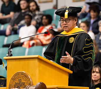
Li received her bachelor’s degree in chemistry from UCLA in 2006. As an undergraduate student, Li conducted research with Professor Tom Mason as well as Professor Fred Hawthorne. Li returned to UCLA in May 2019 to speak to the department’s Careers in Chemistry & Biochemistry class (pictured right).
Li is the fourth UCLA alum to be named to C&EN’s Talented Twelve list. Professor Luis Campos Ph.D. ’06, now a faculty member at Columbia University, was honored in 2016. UCLA Chemistry & Biochemistry faculty members, two of whom are UCLA alums, have been honored – Professor Hosea Nelson was in the first group of Talented 12 in 2015, Professor Alexander Spokoyny ‘06 was honored in 2016, and Professor Jose Rodriguez ’07, Ph.D. ’12, was honored in 2018.
From Chemical & Engineering News (by Matt Davenport):
C&EN’s Talented Twelve – Tina Li 
Credit: Courtesy of Tina Li/Cabot Microelectronics Corporation/Shutterstock/C&EN
Planarization pro is pushing microelectronics to new limits
Tina Li would forgive you if you thought chemical-mechanical planarization, or CMP, was easy. It’s basically a fancy name for polishing.
But it’s polishing with nearly atomic-level precision. Because of that, it has become massively important to the semiconductor industry—to the tune of nearly $2 billion in 2017, according to Linx Consulting—but it’s also rife with chemical challenges.
“CMP sounds like a very simple process, but it’s quite complex,” Li says. “We’re trying to control chemical reactions at the angstrom level.”
“Trying,” however, might be a bit of an understatement. Li’s been helping Cabot Microelectronics Corporation (CMC) remain at the forefront of CMP, rocketing through the company’s ranks and helping launch 10 new products since joining in 2013. And CMC’s clients—the Intels and Samsungs of the world—are using those products as they develop advanced electronics for things like artificial intelligence and autonomous vehicles.
The chips used in these and more pedestrian applications (in our computers and smartphones, for example) consist of multiple layers of electrical insulators, conductors, and semiconductors machined with mind-blowing precision. And the interface between each layer is no exception. Manufacturers want those layers smooth at the subnanometer level.
That’s a huge ask for a polishing slurry that uses a mixture of abrasion and chemical reactions to flatten, or planarize, a surface. Inadvertent dings and scratches can compromise an entire device. In fact, people thought IBM was reckless for first pursuing CMP back in 1983 when a chip’s features were measured in micrometers.
But the process works with the proper chemistry. And as electronics shrink, chemists have become more creative to keep up with the task. Take Li’s early work at CMC. She developed a slurry for polishing silicon oxide using nanoparticles made from cerium oxide, or ceria. This slurry is “softer” than its silica-based predecessor, meaning it relies more on the reactivity of the ceria than its mechanical grit, Li explains.
Her team tuned that reactivity such that the slurry polishes only silicate glass. The slurry stops polishing once it reaches the underlying silicon nitride on a chip, leaving a pristine surface once the slurry is cleaned away. The slurry boasted a best-in-class defectivity—meaning fewer defects—while needing only 0.2% solids by weight. The silica-based predecessor used 12.5%.
Li’s scientific prowess wasn’t the only thing that stood out early at CMC. Her ability to lead was clear, too, which is remarkable for anyone in their early career in the fast-paced semiconductor industry, says Phil Carter, the company’s director of slurry development. The typical product development timeline is roughly 18–24 months.
Li became the youngest R&D manager at CMC in 2015 and recently earned a promotion to the company’s director-level leadership. She’s overseeing an international team that engages directly with customers to understand their technical wants and needs. “She’s codeveloped the technology. She’s delivered the technology. Now she’s helping others do the same,” Carter says.
VITALS
Current affiliation: Cabot Microelectronics
Age: 34
PhD alma mater: Northwestern University
Role model: “For most of my life, my father has worked tirelessly to develop drugs to cure cancer. He has been a shining light for me, and he has continued to grow and evolve, keeping an open mind and fearlessly facing new challenges.”
If I weren’t a chemist, I would be: “I’ve always had an appreciation for building design. I can envision a career as an architectural engineer that would allow me to tap into my love of math and materials chemistry.”
Must-have in the lab: “A particle-size-distribution analyzer to characterize new slurry designs.”
Must-have on the road: “Sneakers.”
Research at a Glance:
Li tuned the chemistry of slurries to—at the angstrom level—polish specific materials on semiconductor devices, work that allows chip manufacturers to make smaller, more powerful electronics.

THREE KEY PAPERS
(J. Phys. Chem. C 2011, DOI: 10.1021/jp112139h)
“Electronic Tuning of Nickel-Based Bis(dicarbollide) Redox Shuttles in Dye-Sensitized Solar Cells”
(Angew. Chem., Int. Ed. 2010, DOI: 10.1002/anie.201002181)
(J. Am. Chem. Soc. 2010, DOI: 10.1021/ja100396n)
The full C&EN article about the Talented Twelve is available here.